 |
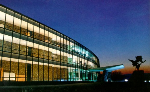
IBM Labs, Yorktown Heights, New York, USA.
Courtesy of IBM |
| |
Yorktown Heights, NY, USA - June 10, 2011
Today,
IBM Research scientists announced that they have achieved a
milestone in creating a building block for the future of wireless devices.
In a paper published yesterday in the magazine Science, IBM researchers announced the first integrated circuit fabricated from wafer-size graphene, and demonstrated a broadband frequency mixer operating at frequencies up to 10 gigahertz (10 billion cycles/second).
Designed for wireless communications, this graphene-based analog integrated circuit could improve today's wireless devices and points to the potential for a new set of applications.
 |
|
IBM Labs, Yorktown Heights, New York, USA.
Courtesy of IBM
|
| |
At today's
conventional frequencies,
cell phone and
transceiver signals could be improved, potentially allowing
phones to work where they can't today while, at
much higher frequencies, military and
medical personnel could see concealed weapons or conduct medical imaging without the same radiation dangers of X-rays.
Graphene, the thinnest electronic material consisting of a single layer of carbon atoms packed in a honeycomb structure, possesses outstanding electrical, optical, mechanical and thermal properties that could make it less expensive and use less energy inside portable electronics like smart phones.
 |
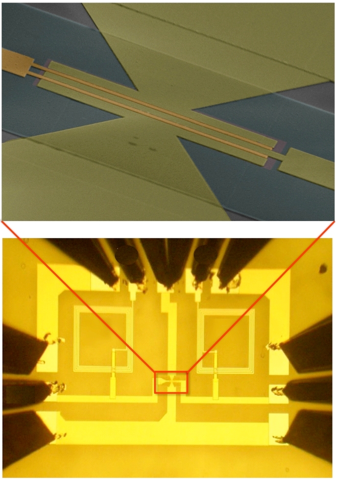
Optical image of a completed graphene integrated circuit (IC) including contact pads.
Courtesy of IBM |
| |
Despite significant scientific progress in the understanding of this novel material and the demonstration of
high-performance graphene-based devices, the challenge of
integrating graphene transistors with other components on a single chip had not been realized until now, mostly due to poor adhesion of
graphene with metals and
oxides and the lack of reliable fabrication schemes to yield reproducible devices and circuits.
This new integrated circuit, consisting of a graphene transistor and a pair of inductors compactly integrated on a silicon carbide (SiC) wafer, overcomes these design hurdles by developing
wafer-scale fabrication procedures that maintain the
quality of graphene and, at the same time, allow for its integration to other components in a
complex circuitry.
 |
Dr. Tze-chiang (T.C.) Chen, Vice President, Science and Technology, IBM Research.
Courtesy of IBM |
| |
“Just a few days before IBM commemorates its 100th anniversary, our scientists have achieved a nanotechnology milestone which continues the company's century-long pursuit of innovation and technology leadership,” said
Dr. T.C. Chen, vice president, Science and Technology, IBM Research.
“This research breakthrough has the potential to in-crease the performance of communication devices that enable people to interact with greater efficiency.”
The breakthrough is also a major milestone for the Carbon Electronics for RF Applications (CERA) program, funded by DARPA.
How it Works
In this demonstration, graphene is synthesized by thermal annealing of SiC wafers to form uniform graphene layers on the surface of SiC.
The fabrication of graphene circuits involves four layers of metal and
two layers of oxide to form
top-gated graphene transistor, on-chip inductors and interconnects.
The circuit operates as a
broadband frequency mixer, which produces output signals with mixed frequencies (sum and difference) of the input signals.
Mixers are fundamental components of many electronic communication systems.
Frequency mixing up to 10 GHz and excellent thermal stability up to 125°C has been demonstrated with the graphene integrated circuit.
 |
Nanotechnology is an enabling technology that is expected to spark advances in various fields. These include advanced functional materials, sensing, tools, healthcare, bio-analytics, water purification, energy technology, and more.
IBM scientists apply their nanoscience expertise to problems outside of nanoelectronics and help tackle some of the biggest challenges of our time, such as more efficient use of solar energy, and new ways of purifying or desalinating water.
Courtesy of IBM |
| |
The fabrication scheme developed can also be applied to other types of graphene materials, including chemical vapor deposited (CVD) graphene films synthesized on metal films, and are also compatible with optical lithography for reduced cost and throughput.
Previously, the team has demonstrated standalone
graphene transistors with a cut-off frequency as high as
100 GHz and
155 GHz for
epitaxial and
CVD graphene, for a
gate length of 240 and 40 nm, respectively.
IBM and Nanotechnology Leadership
In the company's 100 year history, IBM has invested in scientific research to shape the future of computing.
Today's announcement is a demonstration of the results garnered by IBM's world-leading scientists and the company's continual investment in and focus on exploratory research.
Nanotechnology is an enabling technology that is expected to spark advances in various fields.
These include advanced functional materials, sensing, tools, healthcare, bio-analytics, water purification, energy technology, and more.
IBM scientists apply their nanoscience expertise to problems outside of nanoelectronics and help tackle some of the
biggest challenges of our time, such as more efficient use of solar energy, and new ways of purifying or desalinating water.
IBM also recently opened the
Binnig and Rohrer Nanotechnology Center - a facility for world-class nanoscale research recently opened on the campus of IBM Research – Zurich.
The building is the centerpiece of a
10-year strategic partnership in nanoscience between IBM and ETH Zurich, one of Europe's premier technical universities, where scientists will
research novel nanoscale structures and
devices to advance energy and in-formation technologies.
Contact information
Ari Entin
IBM Communications
(408) 927-2272
aentin@us.ibm.com
Source: IBM
http://www-03.ibm.com/press/us/en/pressrelease/34726.wss
ASTROMAN magazine
 subskrypcja RSS