Zurich, Switzerland - June 30, 2011 - For the first time, scientists at IBM Research (NYSE: IBM) have demonstrated that a relatively new memory technology, known as phase-change memory (PCM), can reliably store multiple data bits per cell over extended periods of time. This significant improvement advances the development of low-cost, faster and more durable memory applications for consumer devices, including mobile phones and cloud storage, as well as high-performance applications, such as enterprise data storage.
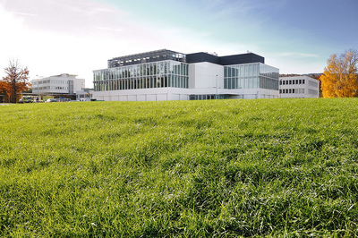 |
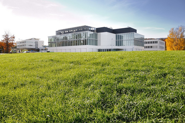
Nanotechnology Center in Rüschlikon. A Unique Public/Private Partnership - the Nanotechnology Center on the campus of IBM Research - Zurich.
For the first time in Switzerland, industry (IBM) and academia (ETH Zurich) will create a research infrastructure for innovative cooperation in a joint effort.
Courtesy of IBM Research – Zurich |
| |
Zurich, Switzerland - June 30, 2011
For the first time, scientists at IBM Research (NYSE: IBM) have demonstrated that a relatively new memory technology, known as phase-change memory (PCM), can reliably store multiple data bits per cell over extended periods of time.
 |
Nanotechnology Center in Rüschlikon.
For the first time in Switzerland, industry (IBM) and academia (ETH Zurich) will create a research infrastructure for innovative cooperation in a joint effort.
Courtesy of IBM Research – Zurich |
| |
This significant improvement advances the development of low-cost, faster and more durable memory applications for consumer devices, including mobile phones and cloud storage, as well as high-performance applications, such as enterprise data storage.
 |
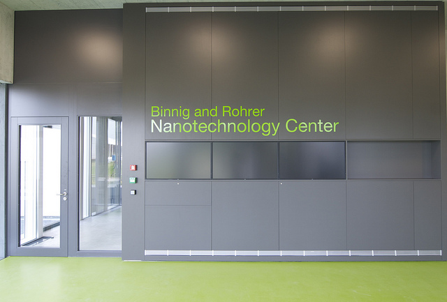
The front lobby of the Binnig and Rohrer Nanotechnology Center, which was dedicated to IBM Fellows and Nobel Laureates Gerd Binnig and Heinrich Rohrer on 17 May 2011.
The two scientists invented the scanning tunneling microscope at the Zurich Research Lab in 1981, thus enabling researchers to see atoms on a surface for the first time.
The Center is the centerpiece of a 10-year strategic partnership in nanoscience between IBM and ETH Zurich where scientists will research novel nanoscale structures and devices for enhancing information technologies.
Courtesy of IBM Research – Zurich / Michael Lowry |
| |
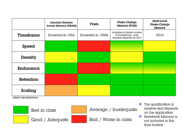
With a combination of speed, endurance, non-volatility and density, PCM can enable a paradigm shift for enterprise IT and storage systems within the next five years.
 |
Heat recovery windows and the façade of the new Nanotechnology Center on the campus of IBM Research - Zurich.
Courtesy of IBM Research – Zurich / BGS Architekten |
| |
Scientists have long been searching for a universal, non-volatile memory technology with far superior performance than flash – today's most ubiquitous non-volatile memory technology.
 |
Prof. Dr. Rolf Eicher, President, ETH Zürich.
Courtesy of IBM Research – Zurich / Gerry Amstutz, ETH Zurich |
| |
The benefits of such a memory technology would allow computers and servers to boot instantaneously and significantly enhance the overall performance of IT systems.
 |
Prof. Dr. Andreas Stemmer, Professor for Nanotechnology, ETH Zürich.
Courtesy of IBM Research – Zurich / Giulia Marthaler, ETH Zurich |
| |
A promising contender is PCM that can write and retrieve data 100 times faster than flash, enable high storage capacities and not lose data when the power is turned off.
 |
Dr. John Kelly, senior vice president, IBM Research, comments,
"Innovation today doesn't occur in silos. It occurs across disciplines and between nations."
Courtesy of IBM Research – Zurich |
| |
Unlike flash, PCM is also very durable and can endure at least 10 million write cycles, compared to current enterprise-class flash at 30,000 cycles or consumer-class flash at 3,000 cycles.
 |
Dr. Matthias Kaiserswerth, Director and Vice President IBM Research – Zurich.
In June 2006 Matthias Kaiserswerth was named director of IBM Research – Zurich, one of nine IBM Research labs worldwide.
Courtesy of IBM Research – Zurich |
| |
While 3,000 cycles will out live many consumer devices, 30,000 cycles are orders of magnitude too low to be suitable for enterprise applications.
 |
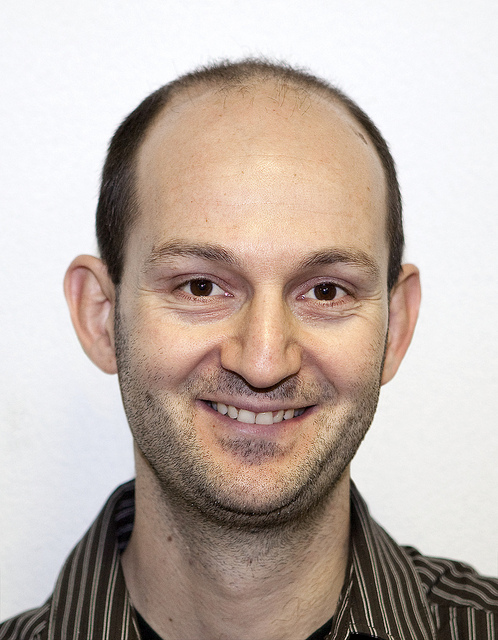
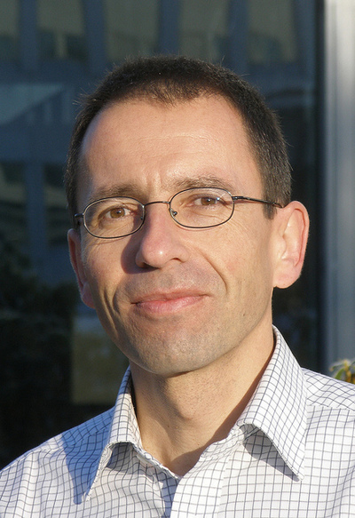
Dr. Haris Pozidis, Manager of Memory and Probe Technologies at IBM Research – Zurich.
For the first time, scientists at IBM Research have demonstrated that a relatively new memory technology, known as phase-change memory (PCM), can reliably store multiple data bits per cell over extended periods of time.
This significant improvement advances the development of low-cost, faster and more durable memory applications for consumer devices, including mobile phones and cloud storage, as well as high-performance applications, such as enterprise data storage.
Courtesy of IBM Research – Zurich |
| |
"As organizations and consumers increasingly embrace cloud-computing models and services, whereby most of the data is stored and processed in the cloud, ever more powerful and efficient, yet affordable storage technologies are needed," states Dr. Haris Pozidis, Manager of Memory and Probe Technologies at IBM Research – Zurich.
"By demonstrating a multi-bit phase-change memory technology which achieves for the first time reliability levels akin to those required for enterprise applications, we made a big step towards enabling practical memory devices based on multi-bit PCM."
Multi-level Phase Change Memory Breakthrough
To achieve this breakthrough demonstration, IBM scientists in Zurich used advanced modulation coding techniques to mitigate the problem of short-term drift in multi-bit PCM, which causes the stored resistance levels to shift over time, which in turn creates read errors.
 |
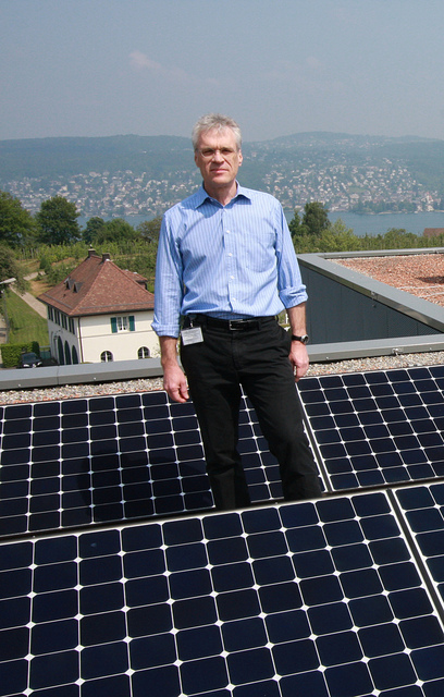
Dr. Paul Seidler, Coordinator of the Nanotechnology Center at IBM Research – Zurich.
Courtesy of IBM Research – Zurich / Jos Schmid |
| |
Up to now, reliable retention of data has only been shown for single bit-per-cell PCM, whereas no such results on multi-bit PCM have been reported.
 |
Dr. Paul Seidler, coordinator for the Nanotechnology Center at IBM Research - Zurich stands on the roof of the cutting edge laboratory, which is covered in solar panels.
The Nanotechnology Center will continue IBM's tradition of environmental awareness and has been granted the use of the MINERGIE standard quality label. MINERGIE status is granted to new and refurbished low-energy-consumption buildings in Switzerland.
To reach this standard, IBM is utilizing several innovations including:
- Photovoltaic power system
- Geothermal heat exchange system
- Heat recovery windows and cutting-edge climate systems.
The roof of the underground garage at the Nanotechnology Center features a special layer of stones, sand and earth which will provide a new habitat for a variety of native plants, reptiles and insects.
Courtesy of IBM Research – Zurich / Michael Lowry |
| |
PCM leverages the resistance change that occurs in the material - an alloy of various elements - when it changes its phase from crystalline – featuring low resistance – to amorphous – featuring high resistance – to store data bits.
 |
Dr. Walter Riess, Department Head Science and Technology, IBM Research - Zurich.
Courtesy of IBM Research – Zurich / Charlotte Bolliger |
| |
In a PCM cell, where a phase-change material is deposited between a top and a bottom electrode, phase change can controllably be induced by applying voltage or current pulses of different strengths.
 |
A Drift-tolerant coding demonstration by IBM Researchers in Zurich demonstrated the first large-scale demonstration of multi-level cell state retention in phase-change memory.
Courtesy of IBM Research – Zurich / Michael Lowry |
| |
These heat up the material and when distinct temperature thresholds are reached cause the material to change from crystalline to amorphous or vice versa.
 |
Scientists have long been searching for a universal, non-volatile memory technology with far superior performance than Flash – today’s most ubiquitous non-volatile memory technology.
The benefits of such a memory technology would allow computers and servers to boot instantaneously and significantly enhance the overall performance of IT systems.
A promising contender is PCM that can write and retrieve data 100 times faster than Flash, enable high storage capacities and not lose data when the power is turned off. Unlike Flash, PCM is also very durable and can endure at least 10 million write cycles, compared to current enterprise-class Flash at 30,000 cycles or consumer-class Flash at 3,000 cycles.
While 3,000 cycles will out live many consumer devices, 30,000 cycles are orders of magnitude too low to be suitable for enterprise applications.
Courtesy of IBM Research |
| |
In addition, depending on the voltage, more or less material between the electrodes will undergo a phase change, which directly affects the cell's resistance.
 |
Dr. Roland Germann, Manager Nanotechnology Center Operations at IBM Research – Zurich.
Courtesy of IBM Research – Zurich / Charlotte Bolliger |
| |
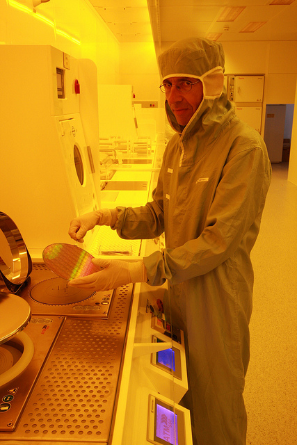
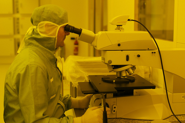
Scientists exploit that aspect to store not only one bit, but multiple bits per cell.
 |
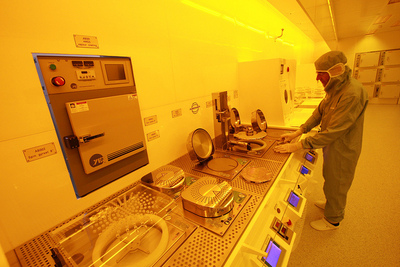
Dr. Roland Germann, manager, Nanotechnology Center Operations at IBM Research - Zurich in the clean room with a silicon wafer.
The Nanotechnology Center includes class 100 (ISO 5) to class 10'000 (ISO 7) cleanroom facilities, including lithography for pattern definition; wet processing for substrate cleaning and wet chemical etching; thin-film deposition of metals and insulators; dry etching for material removal using reactive gases; thermal processing for oxidation and annealing; vapor phase deposition; backend processes such as plating, lapping/polishing, dicing and bonding; and polymer waveguide processing for optical interconnects.
Processes, most of which will be semiconductor-based (wafer sizes up to 200mm), will be conducted on materials similar to those used in standard semiconductor technology, such as silicon, metals, insulators, polymers, organics and oxides.
Courtesy of IBM Research – Zurich / Michael Lowry |
| |
In the present work, IBM scientists used four distinct resistance levels to store the bit combinations "00", "01" 10" and "11".
 |
The Nanotechnology Center includes class 100 (ISO 5) to class 10'000 (ISO 7) cleanroom facilities, including lithography for pattern definition; wet processing for substrate cleaning and wet chemical etching; thin-film deposition of metals and insulators; dry etching for material removal using reactive gases; thermal processing for oxidation and annealing; vapor phase deposition; backend processes such as plating, lapping/polishing, dicing and bonding; and polymer waveguide processing for optical interconnects.
Processes, most of which will be semiconductor-based (wafer sizes up to 200mm), will be conducted on materials similar to those used in standard semiconductor technology, such as silicon, metals, insulators, polymers, organics and oxides.
Courtesy of IBM Research – Zurich / Michael Lowry |
| |
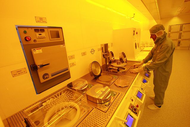
To achieve the demonstrated reliability, crucial technical advancements in the " read" and " write" process were necessary.
 |
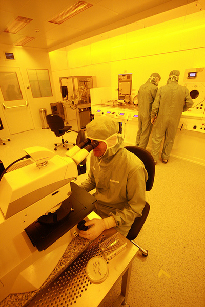
A 100 mm wafer on a hotplate in the lithography sector.
The Nanotechnology Center includes class 100 (ISO 5) to class 10'000 (ISO 7) cleanroom facilities, including lithography for pattern definition; wet processing for substrate cleaning and wet chemical etching; thin-film deposition of metals and insulators; dry etching for material removal using reactive gases; thermal processing for oxidation and annealing; vapor phase deposition; backend processes such as plating, lapping/polishing, dicing and bonding; and polymer waveguide processing for optical interconnects.
Processes, most of which will be semiconductor-based (wafer sizes up to 200mm), will be conducted on materials similar to those used in standard semiconductor technology, such as silicon, metals, insulators, polymers, organics and oxides.
Courtesy of IBM Research – Zurich / Michael Lowry |
| |
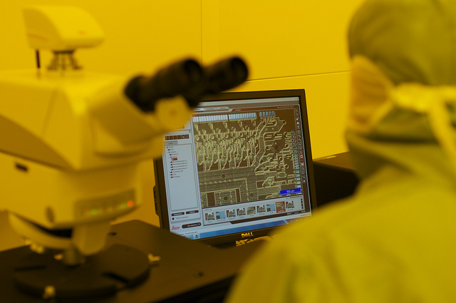
The scientists implemented an iterative " write" process to overcome deviations in the resistance due to inherent variability in the memory cells and the phase-change materials:
"We apply a voltage pulse based on the deviation from the desired level and then measure the resistance. If the desired level of resistance is not achieved, we apply another voltage pulse and measure again – until we achieve the exact level," explains Pozidis.
 |
The Nanotechnology Center includes class 100 (ISO 5) to class 10'000 (ISO 7) cleanroom facilities, including lithography for pattern definition; wet processing for substrate cleaning and wet chemical etching; thin-film deposition of metals and insulators; dry etching for material removal using reactive gases; thermal processing for oxidation and annealing; vapor phase deposition; backend processes such as plating, lapping/polishing, dicing and bonding; and polymer waveguide processing for optical interconnects.
Processes, most of which will be semiconductor-based (wafer sizes up to 200mm), will be conducted on materials similar to those used in standard semiconductor technology, such as silicon, metals, insulators, polymers, organics and oxides.
Courtesy of IBM Research – Zurich / Michael Lowry |
| |
Despite using the iterative process, the scientists achieved a worst-case write latency of about 10 microseconds, which represents a 100x performance increase over even the most advanced Flash memory on the market today.
 |
The Nanotechnology Center includes class 100 (ISO 5) to class 10'000 (ISO 7) cleanroom facilities, including lithography for pattern definition; wet processing for substrate cleaning and wet chemical etching; thin-film deposition of metals and insulators; dry etching for material removal using reactive gases; thermal processing for oxidation and annealing; vapor phase deposition; backend processes such as plating, lapping/polishing, dicing and bonding; and polymer waveguide processing for optical interconnects.
Processes, most of which will be semiconductor-based (wafer sizes up to 200mm), will be conducted on materials similar to those used in standard semiconductor technology, such as silicon, metals, insulators, polymers, organics and oxides.
Courtesy of IBM Research – Zurich / Michael Lowry |
| |
For demonstrating reliable read-out of data bits, the scientists needed to tackle the problem of resistance drift.
Because of structural relaxation of the atoms in the amorphous state, the resistance increases over time after the phase change, eventually causing errors in the read-out.
To overcome that issue, the IBM scientists applied an advanced modulation coding technique that is inherently drift-tolerant.
The modulation coding technique is based on the fact that, on average, the relative order of programmed cells with different resistance levels does not change due to drift.
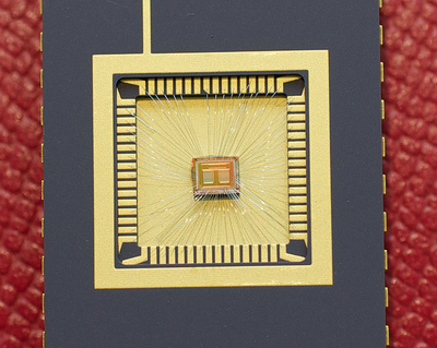
Using that technique, the IBM scientists were able to mitigate drift and demonstrate long- term retention of bits stored in a subarray of 200,000 cells of their PCM test chip, fabricated in 90-nanometer CMOS technology.
 |
The Nanotechnology Center includes class 100 (ISO 5) to class 10'000 (ISO 7) cleanroom facilities, including lithography for pattern definition; wet processing for substrate cleaning and wet chemical etching; thin-film deposition of metals and insulators; dry etching for material removal using reactive gases; thermal processing for oxidation and annealing; vapor phase deposition; backend processes such as plating, lapping/polishing, dicing and bonding; and polymer waveguide processing for optical interconnects.
Processes, most of which will be semiconductor-based (wafer sizes up to 200mm), will be conducted on materials similar to those used in standard semiconductor technology, such as silicon, metals, insulators, polymers, organics and oxides.
Courtesy of IBM Research – Zurich / Michael Lowry |
| |
The PCM test chip was designed and fabricated by scientists and engineers located in Burlington, Vermont; Yorktown Heights, New York and in Zurich.
This retention experiment has been under way for more than five months, indicating that multi-bit PCM can achieve a level of reliability that is suitable for practical applications.
The PCM research project at IBM Research – Zurich will continue to be studied at the recently opened Binnig and Rohrer Nanotechnology Center.
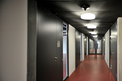
The center, which is jointly operated by IBM and ETH Zurich as part of a strategic partnership in nanosciences, offers a cutting-edge infrastructure, including a large cleanroom for micro- and nanofabrication as well as six "noise-free" labs, especially shielded laboratories for highly sensitive experiments.
A History of Pioneering Memory Technology
IBM has a history in creating breakthrough computer memory technology.
In 1966, IBM Fellow, Dr. Robert Dennard invented dynamic random access memory - DRAM - which, when combined with the first low-cost microprocessors, opened the door to small personal computers.
Today, every PC, notebook computer, game console and other computing device is loaded with DRAM chips.
DRAM also powers mainframes, data center servers and most of the machines that run the Internet.
In 1988, Dr. Dennard was awarded the US National Medal of Technology for the invention of DRAM.
As IBM commemorates its Centennial this year, the company celebrates DRAM as one of its 100 greatest innovations.
For more information, visit:
http://www.ibm.com/ibm100/us/en/icons/dram/
The paper " Drift-tolerant Multilevel Phase-Change Memory" by N. Papandreou, H. Pozidis, T. Mittelholzer, G.F. Close, M. Breitwisch, C. Lam and E. Eleftheriou, was recently presented by Haris Pozidis at the 3rd IEEE International Memory Workshop in Monterey, CA.
Contacts information
Ari Entin
IBM Media Relations
+1 408 927 2274
aentin@us.ibm.com
Chris Sciacca
IBM Media Relations
+41 44 724 84 43
cia@zurich.ibm.com
Source: IBM
http://www-03.ibm.com/press/us/en/pressrelease/34949.wss
ASTROMAN Magazine – 2011.06.17
IBM's Watson Computing System Honored as "Person of the Year"
http://www.astroman.com.pl/index.php?mod=magazine&a=read&id=998
ASTROMAN Magazine – 2011.06.12
IBM Scientists Build the First Wafer-Scale Graphene Integrated Circuit Smaller than a Pinhead
http://www.astroman.com.pl/index.php?mod=magazine&a=read&id=995
ASTROMAN Magazine – 2011.06.02
IBM Helps City of Fort Worth and Tarrant County Create a Smarter Public Safety System
http://www.astroman.com.pl/index.php?mod=magazine&a=read&id=985
ASTROMAN Magazine – 2011.05.15
ICM Selects IBM to Fuel National Science
http://www.astroman.com.pl/index.php?mod=magazine&a=read&id=973
ASTROMAN Magazine – 2011.05.08
IBM Commemorates NASA's 50th Anniversary of First U.S. Manned Space Flight
http://www.astroman.com.pl/index.php?mod=magazine&a=read&id=967
ASTROMAN Magazine – 2011.05.01
Yale School of Management and IBM Collaborate to Prepare Students for the Next Generation of Jobs
http://www.astroman.com.pl/index.php?mod=magazine&a=read&id=961
ASTROMAN Magazine – 2011.04.21
IBM Reports 2011 First-Quarter Results
http://www.astroman.com.pl/index.php?mod=magazine&a=read&id=950
ASTROMAN Magazine – 2011.03.18
IBM już od 18 lat najbardziej innowacyjną firmą świata
http://www.astroman.com.pl/index.php?mod=magazine&a=read&id=919
ASTROMAN Magazine – 2011.02.20
IBM to Collaborate with Nuance to Apply IBM's "Watson" Analytics Technology to Healthcare
http://www.astroman.com.pl/index.php?mod=magazine&a=read&id=899
ASTROMAN Magazine – 2011.02.20
IBM "Watson" to Challenge Humans at Jeopardy!
http://www.astroman.com.pl/index.php?mod=magazine&a=read&id=898
ASTROMAN Magazine – 2010.12.25
IBM's "Watson" Computing System to Challenge All Time Greatest Jeopardy! Champions
http://www.astroman.com.pl/index.php?mod=magazine&a=read&id=864
ASTROMAN magazine
|
 subskrypcja RSS