Armonk, N.Y., and Santa Clara, Calif., USA - October 20, 2014 - IBM (NYSE: IBM) and GLOBALFOUNDRIES today announced that they have signed a Definitive Agreement under which GLOBALFOUNDRIES plans to acquire IBM's global commercial semiconductor technology business, including intellectual property, world-class technologists and technologies related to IBM Microelectronics, subject to completion of applicable regulatory reviews. GLOBALFOUNDRIES will also become IBM's exclusive server processor semiconductor technology provider for 22 nanometer (nm), 14nm and 10nm semiconductors for the next 10 years. The Agreement, once closed, enables IBM to further focus on fundamental semiconductor research and the development of future cloud, mobile, big data analytics, and secure transaction-optimized systems. IBM continues its previously announced $3 billion investment over five years for semiconductor technology research to lead in the next generation of computing. GLOBALFOUNDRIES will have primary access to the research that results from this investment through joint collaboration at the Colleges of Nanoscale Science and Engineering (CNSE), SUNY Polytechnic Institute, in Albany, N.Y.
 |
IBM and GLOBALFOUNDRIES signed a definitive agreement under which GLOBALFOUNDRIES will acquire IBM's global commercial semiconductor technology business, while IBM sharpens its focus on semiconductor and material science research, development capabilities and leadership in high-value systems.
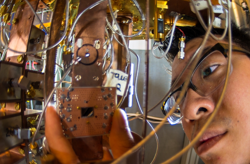
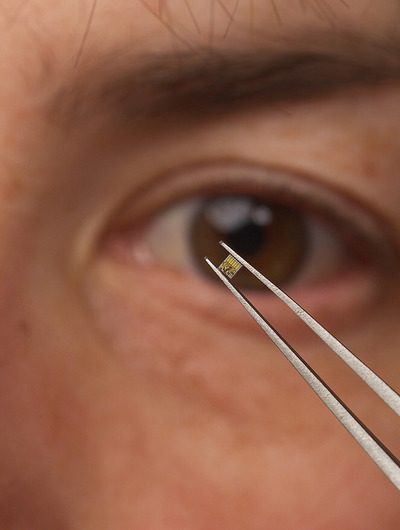
IBM scientists, including researcher Jerry Chow (pictured), are exploring post-silicon semiconductor materials, such as carbon nanoelectronics, silicon photonics, new memory technologies, and architectures to meet the emerging demands of cloud, Big Data and secure transaction optimized systems.
Photo courtesy of IBM Research/Jon Simon |
| |
Armonk, N.Y., and Santa Clara, Calif., USA - October 20, 2014
• Acquisition Enables GLOBALFOUNDRIES to Become a World Leader in Semiconductor Foundry Technology
• IBM to Focus on Fundamental Semiconductor Research and Systems Innovation
IBM (NYSE: IBM) and GLOBALFOUNDRIES today announced that they have signed a Definitive Agreement under which GLOBALFOUNDRIES plans to acquire IBM's global commercial semiconductor technology business, including intellectual property, world-class technologists and technologies related to IBM Microelectronics, subject to completion of applicable regulatory reviews.
 |
Graphene Integrated Circuit
In 2011, IBM Research scientists announced that they have achieved a milestone in creating a building block for the future of wireless devices. In a paper published yesterday in the magazine Science, IBM researchers announced the first integrated circuit fabricated from wafer-size graphene, and demonstrated a broadband frequency mixer operating at frequencies up to 10 gigahertz (10 billion cycles/second).
Photo courtesy of IBM Research |
| |
GLOBALFOUNDRIES will also become IBM's exclusive server processor semiconductor technology provider for 22 nanometer (nm), 14nm and 10nm semiconductors for the next 10 years.
The Agreement, once closed, enables IBM to further focus on fundamental semiconductor research and the development of future cloud, mobile, big data analytics, and secure transaction-optimized systems.
 |
In 2005, IBM announced the availability of its fourth generation silicon germanium foundry technology, named 8HP - with over 2X performance of the previous generation.
The new 130 nanometer (nm) silicon germanium (SiGe) bipolar complementary metal oxide semiconductor (BiCMOS) foundry technology can reduce the cost of mobile consumer products, advance high-bandwidth wireless communications, and help enable innovative new applications such as collision-avoidance automobile radar.
Photo courtesy of IBM Research |
| |
IBM continues its previously announced $3 billion investment over five years for semiconductor technology research to lead in the next generation of computing.
GLOBALFOUNDRIES will have primary access to the research that results from this investment through joint collaboration at the Colleges of Nanoscale Science and Engineering (CNSE), SUNY Polytechnic Institute, in Albany, N.Y.
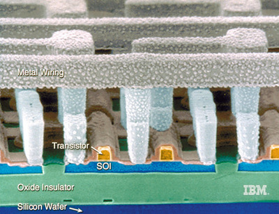 |
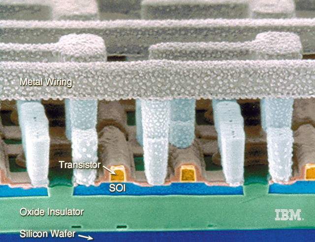
Silicon On Insulator (SOI) chip 2007
At the annual Design Automation Conference in 2007, IBM announced new semiconductor products that leverage several IBM-generated chip technology breakthroughs.
One of these offerings, IBM's new Cu-45 High Performance Custom Chip (ASIC), represents the commercial introduction of Silicon On Insulator (SOI) technology - historically only used for high performance microprocessors - into communications, consumer and other major market segments.
In addition, the Cu-45HP ASIC offering is the first commercial use of a new generation of embedded dynamic random access memory (eDRAM) implemented in Silicon-on-Insulator (SOI) technology - an innovation introduced February 2007 at the International Solid State Circuits Conference (ISSCC).
Photo courtesy of IBM Research |
| |
As part of this Agreement, GLOBALFOUNDRIES will gain substantial intellectual property including thousands of patents, making GLOBALFOUNDRIES the holder of one of the largest semiconductor patent portfolios in the world.
 |
Scientists Discover New Atomic Technique to Charge Memory Chips 2013.
In 2013, IBM announced a materials science breakthrough at the atomic level that could pave the way for a new class of non-volatile memory and logic chips that would use less power than today’s silicon based devices.
Rather than using conventional electrical means that operate today’s semiconducting devices, IBM’s scientists discovered a new way to operate chips using tiny ionic currents, which are streams of charged atoms that could mimic the event-driven way in which the human brain operates.
Photo courtesy of IBM Research |
| |
GLOBALFOUNDRIES also will benefit from an influx of one of the best technical teams in the semiconductor industry, which will solidify its path to advanced process geometries at 10nm and below.
Additionally, the acquisition opens up business opportunities in industry-leading radio frequency (RF) and specialty technologies and ASIC design capabilities.
 |
IBM CMOS Integrated Silicon Nanophotonics Technology.
IBM's new CMOS Integrated Silicon Nanophotonics chip technology integrates electrical and optical devices on the same piece of silicon, enabling computer chips to communicate using pulses of light (instead of electrical signals).
Photo courtesy of IBM Research |
| |
"This acquisition solidifies GLOBALFOUNDRIES' leadership position in semiconductor technology development and manufacturing,” said Dr. Sanjay Jha, CEO, GLOBALFOUNDRIES.
“We can now offer our customers a broader range of differentiated leading-edge 3D transistor and RF technologies, and we will also improve our design ecosystem to accelerate time-to-revenue for our customers. This acquisition further strengthens advanced manufacturing in the United States, and builds on established relationships in New York and Vermont.”
 |
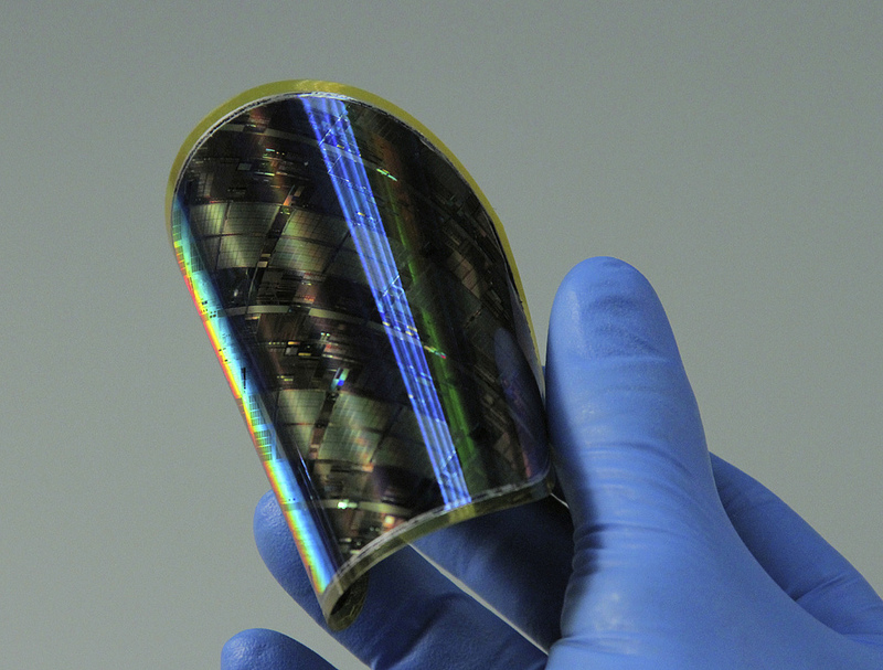
Flexible nanoscale circuits 2
Mighty electronic chips in your clothes to monitor your vitals?
A tablet that folds up and fits in your back pocket?
Research scientists Stephen Bedell and Davood Shahrjerdi at IBM's Thomas J Watson Research Center in Yorktown Heights, New York think that flexible nanoscale circuits can do just that.
The flexible nanoelectronic circuit Bedell and Shahrjedri designed is 10,000 times thinner than a piece of paper, and was peeled off of a silicon wafer and put onto plastic – an industry first.
These circuits are also easily transferrable at any size, arbitrary in shape, and compatible with any flexible substrate.
With a radius of curvature of only 6 mm, these sheets of circuits could cover or roll on top of almost anything.
The Controlled Spalling Technique that was used to create the flexible circuits can be applied to other materials as well.
For instance, Controlled Spalling could also be used to replace the poor thermal conducting sapphire substrate on solid state lighting. In this application the light (and heat) generating layers can be removed from the sapphire and mounted onto a higher thermally conducting material, such as metal.
Photo courtesy of IBM Research |
| |
“The Agreement expands our longstanding collaboration, which began when GLOBALFOUNDRIES was created in 2009, and reflects our confidence in GLOBALFOUNDRIES’ capability,” said IBM Senior Vice President & Director of Research Dr. John E. Kelly III.
“This acquisition enables IBM to focus on fundamental semiconductor and material science research, development capabilities and expertise in high-value systems, with GLOBALFOUNDRIES' leadership in advanced technology manufacturing at scale and commitment to delivering future semiconductor technologies. We are grateful for the leadership and investments by the states of New York and Vermont in supporting the semiconductor industry.”
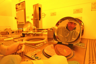 |
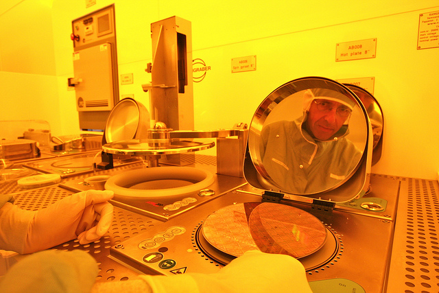
The reflection of Dr. Roland Germann, manager, Nanotechnology Center Operations at IBM Research - Zurich in the clean room with a silicon wafer.
The Nanotechnology Center includes class 100 (ISO 5) to class 10'000 (ISO 7) cleanroom facilities, including lithography for pattern definition; wet processing for substrate cleaning and wet chemical etching; thin-film deposition of metals and insulators; dry etching for material removal using reactive gases; thermal processing for oxidation and annealing; vapor phase deposition; backend processes such as plating, lapping/polishing, dicing and bonding; and polymer waveguide processing for optical interconnects.
Processes, most of which will be semiconductor-based (wafer sizes up to 200mm), will be conducted on materials similar to those used in standard semiconductor technology, such as silicon, metals, insulators, polymers, organics and oxides.
Photo courtesy of IBM Research/Michael Lowry |
| |
This acquisition bolsters semiconductor manufacturing and technology development in the United States.
GLOBALFOUNDRIES has robust capital expenditure plans of approximately $10 billion in 2014-2015, with the majority being invested in New York.
 |
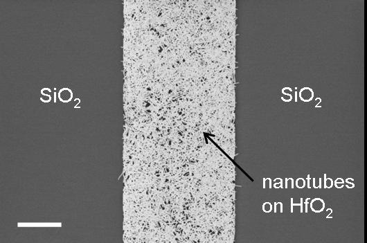
IBM SEM of carbon nanotube substrate
IBM SEM image of carbon nanotubes deposited on a trench coated in hafnium oxide (HfO2) showing extremely high density and excellent selectivity (scale bar: 2 μm).
Photo courtesy of IBM Research |
| |
GLOBALFOUNDRIES has created nearly 3,000 direct jobs in New York and thousands more indirect jobs in the United States since 2009.
GLOBALFOUNDRIES will acquire and operate existing IBM semiconductor manufacturing operations and facilities in East Fishkill, New York and Essex Junction, Vermont, adding capacity to serve its customers and thousands of jobs to GLOBALFOUNDRIES' workforce.
 |
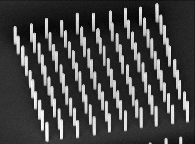
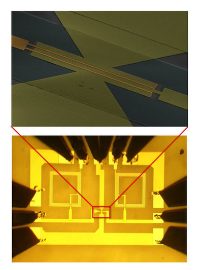
Nanowires
Ecole Polytechnique Fédérale de Lausanne and IBM announced a major research initiative, with several leading academic and corporate research organizations across Europe, to address the alarming growth of energy consumption by electronic devices, ranging from mobile phones to laptops to televisions to supercomputers.
The research project, called Steeper, aims to increase the energy efficiency of these devices, when active, by 10 times and virtually eliminate power consumption when they are in passive or standby mode.
To achieve this, scientists will study the development of so-called TFETs based on silicon (Si), silicon-germanium (SiGe) and III-V semiconducting nanowires (photo).
Nanowires are cylindrical structures measuring only a few nanometers (nm) in diameter, which allow optimum electrostatic control of the transistor channel.
In a TFET quantum mechanical band-to-band tunneling is exploited to switch on the device and thus achieve a steeper turn-on characteristics compared to conventional MOSFETs.
Project Steeper will evaluate the physical and practical limits of boosting the performance of TFETs with III-V nanowires, and the resulting advantages for future energy efficient digital circuits.
InAs nanowires epitaxially grown on top of a silicon substrate using metal-organic chemical vapor deposition.
Spacing between wires is 1 micrometer.
Image courtesy by Mikael Björk, IBM Research – Zurich |
| |
GLOBALFOUNDRIES plans to provide employment opportunities for substantially all IBM employees at the two facilities who are part of the transferred businesses, except for a team of semiconductor server group employees who will remain with IBM.
After the close of this transaction, GLOBALFOUNDRIES will be the largest semiconductor technology manufacturing employer in the Northeast.
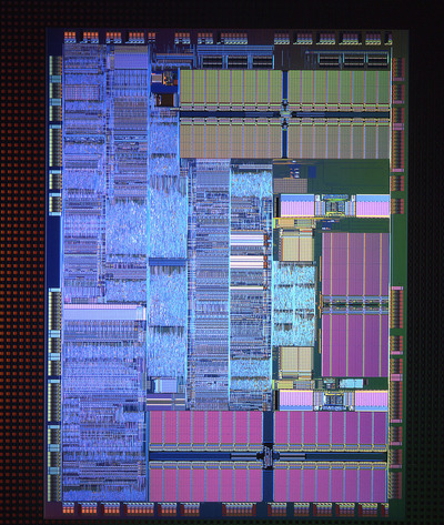 |
Copper Chip Technology
Photo courtesy of IBM Research |
| |
GLOBALFOUNDRIES will also acquire IBM's commercial microelectronics business, which includes ASIC and specialty foundry, manufacturing and related operations and sales. GLOBALFOUNDRIES plans to invest to grow these businesses.
IBM will reflect a pre-tax charge of $4.7 billion in its financial results for the third quarter of 2014, which includes an asset impairment, estimated costs to sell the IBM microelectronics business, and cash consideration to GLOBALFOUNDRIES.
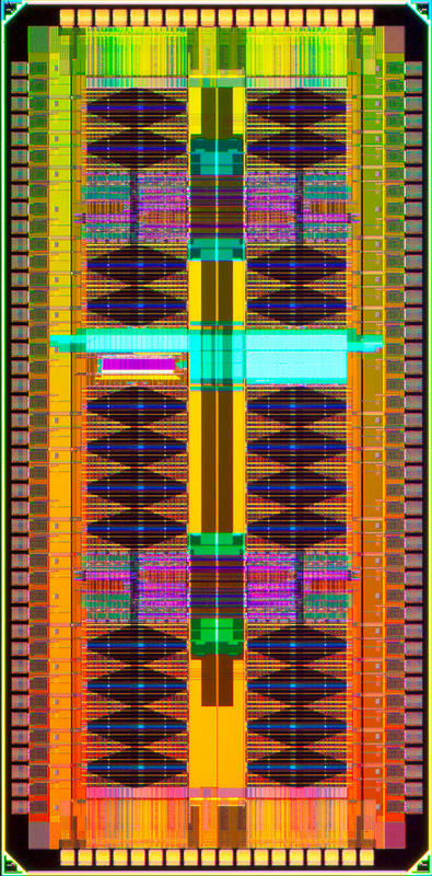 |
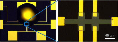
Embedded DRAM
IBM's embedded dynamic random access memory (test chip shown here) will help deliver a thrilling new game experience to Nintendo fans.
The new memory technology, a key element of the new Power microprocessor that IBM is building for the Nintendo NAME TK, can triple the amount of memory contained on a single chip, making for extreme game play.
Photo courtesy of IBM Research |
| |
Cash consideration of $1.5 billion is expected to be paid to GLOBALFOUNDRIES by IBM over the next three years.
The cash consideration will be adjusted by the amount of working capital which is estimated to be $200 million.
The transaction is subject to the satisfaction of regulatory requirements and customary closing conditions.
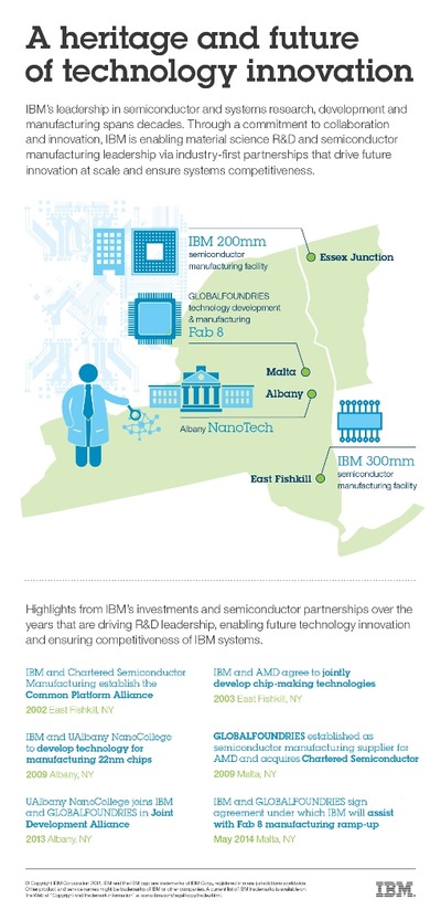 |
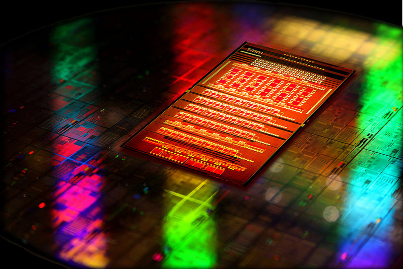
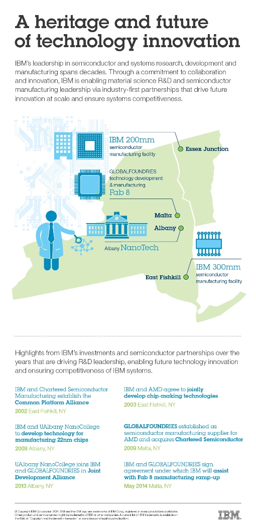
IBM's investments and semiconductor partnerships over the years are driving R&D leadership and enabling future technology innovation to meet the emerging demands of cloud, Big Data, transaction processing and analytics-optimized systems.
Photo courtesy of IBM Research |
| |
About GLOBALFOUNDRIES
GLOBALFOUNDRIES is the world’s first full-service semiconductor foundry with a truly global footprint.
Launched in March 2009, the company has quickly achieved scale as the second largest foundry in the world, providing a unique combination of advanced technology and manufacturing to more than 160 customers.
With operations in Singapore, Germany and the United States, GLOBALFOUNDRIES is the only foundry that offers the flexibility and security of manufacturing centers spanning three continents.
The company’s three 300mm fabs and five 200mm fabs provide the full range of process technologies from mainstream to the leading edge.
This global manufacturing footprint is supported by major facilities for research, development and design enablement located near hubs of semiconductor activity in the United States, Europe and Asia.
GLOBALFOUNDRIES is owned by the Mubadala Development Company.
For more information, visit http://www.globalfoundries.com
About IBM
For more information on IBM, visit http://www.ibm.com
Contacts information
Jeff Cross
IBM Media Relations
1 (914) 766-4166
jrcross@us.ibm.com
Jason Gorss
GLOBALFOUNDRIES
1 (518) 698-7765
Jason.gorss@globalfoundries.com
Chris Andrews
IBM Media Relations
1 (914) 499-4045
candrews@us.ibm.com
Travis Bullard
GLOBALFOUNDRIES
1 (518) 491-7658
travis.bullard@globalfoundries.com
Source: IBM
http://www-03.ibm.com/press/us/en/index.wss
ASTROMAN Magazine - 2014.08.30
IBM Watson Ushers in a New Era of Data-Driven Discoveries
http://www.astroman.com.pl/index.php?mod=magazine&a=read&id=1783
ASTROMAN Magazine - 2014.08.10
Wroclaw University of Technology Delivers Personalized Classrooms on IBM Cloud Infrastructure
http://www.astroman.com.pl/index.php?mod=magazine&a=read&id=1772
ASTROMAN Magazine - 2014.08.02
IBM acquires CrossIdeas to Expand Security Offerings with Identity Intelligence
http://www.astroman.com.pl/index.php?mod=magazine&a=read&id=1767
ASTROMAN Magazine - 2014.07.16
Apple and IBM Forge Global Partnership to Transform Enterprise Mobility
http://www.astroman.com.pl/index.php?mod=magazine&a=read&id=1757
ASTROMAN Magazine - 2014.07.12
IBM Announces $3 Billion Research Initiative to Tackle Chip Grand Challenges for Cloud and Big Data Systems
http://www.astroman.com.pl/index.php?mod=magazine&a=read&id=1755
ASTROMAN Magazine - 2014.07.08
City of Madrid Implements IBM's Large Smarter Cities Environmental Analytics Project
http://www.astroman.com.pl/index.php?mod=magazine&a=read&id=1751
ASTROMAN Magazine - 2014.06.27
Qatar Public Works Authority 'Ashghal' Selects IBM for Smarter Infrastructure
https://www.astroman.com.pl/index.php?mod=magazine&a=read&id=1741
ASTROMAN Magazine - 2014.05.11
Report: IBM Named #1 Preferred Provider of IaaS Cloud by Enterprises
http://www.astroman.com.pl/index.php?mod=magazine&a=read&id=1710
ASTROMAN Magazine – 2014.02.01
IBM and Twitter Announce Patent and Cross-License Agreement. Twitter purchases 900 patents from IBM
http://www.astroman.com.pl/index.php?mod=magazine&a=read&id=1648
ASTROMAN Magazine - 2013.12.22
IBM to Acquire Aspera to Help Companies Speed Global Movement of Big Data
http://www.astroman.com.pl/index.php?mod=magazine&a=read&id=1610
ASTROMAN Magazine - 2013.11.16
IBM Watson's Next Venture: Fueling New Era of Cognitive Apps Built in the Cloud by Developers
http://www.astroman.com.pl/index.php?mod=magazine&a=read&id=1587
ASTROMAN Magazine - 2013.10.26
President Barack Obama to Visit IBM'S P-TECH School in Brooklyn, NY, USA
http://www.astroman.com.pl/index.php?mod=magazine&a=read&id=1576
ASTROMAN Magazine - 2013.09.21
IBM Acquires Daeja Image Systems Ltd.
http://www.astroman.com.pl/index.php?mod=magazine&a=read&id=1557
ASTROMAN Magazine - 2013.09.01
IBM Closes Acquisition of CSL International
http://www.astroman.com.pl/index.php?mod=magazine&a=read&id=1541
ASTROMAN Magazine – 2013.08.17
IBM to Acquire Trusteer to Help Companies Combat Financial Fraud and Advanced Security Threats
http://www.astroman.com.pl/index.php?mod=magazine&a=read&id=1519
ASTROMAN Magazine – 2013.08.17
IBM Awarded 10 Year US$1 Billion Cloud Hosting Services Contract
http://www.astroman.com.pl/index.php?mod=magazine&a=read&id=1518
ASTROMAN Magazine – 2013.04.08
IBM To Open Cloud Lab For Wall Street Clients
http://www.astroman.com.pl/index.php?mod=magazine&a=read&id=1440
ASTROMAN Magazine – 2012.03.03
IBM Forms Watson Healthcare Advisory Board
http://www.astroman.com.pl/index.php?mod=magazine&a=read&id=1191
ASTROMAN Magazine – 2011.11.01
IBM Watson Heads to Harvard, MIT to Explore Future of Technology in Business
http://www.astroman.com.pl/index.php?mod=magazine&a=read&id=1092
ASTROMAN Magazine – 2011.09.12
WellPoint and IBM Announce Agreement to Put Watson to Work in Health Care
http://www.astroman.com.pl/index.php?mod=magazine&a=read&id=1056
ASTROMAN Magazine – 2011.06.17
IBM's Watson Computing System Honored as "Person of the Year"
http://www.astroman.com.pl/index.php?mod=magazine&a=read&id=998
ASTROMAN Magazine – 2011.02.20
IBM to Collaborate with Nuance to Apply IBM's "Watson" Analytics Technology to Healthcare
http://www.astroman.com.pl/index.php?mod=magazine&a=read&id=899
ASTROMAN Magazine – 2011.02.20
IBM "Watson" to Challenge Humans at Jeopardy!
http://www.astroman.com.pl/index.php?mod=magazine&a=read&id=898
ASTROMAN Magazine – 2010.12.25
IBM's "Watson" Computing System to Challenge All Time Greatest Jeopardy! Champions
http://www.astroman.com.pl/index.php?mod=magazine&a=read&id=864
Editor-in-Chief of ASTROMAN magazine: Roman Wojtala, PhD.
|
 subskrypcja RSS