|
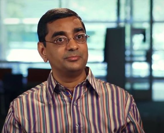
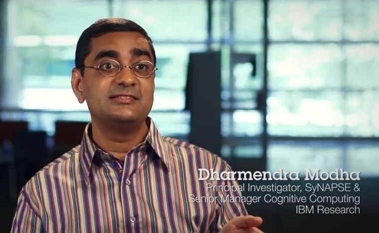
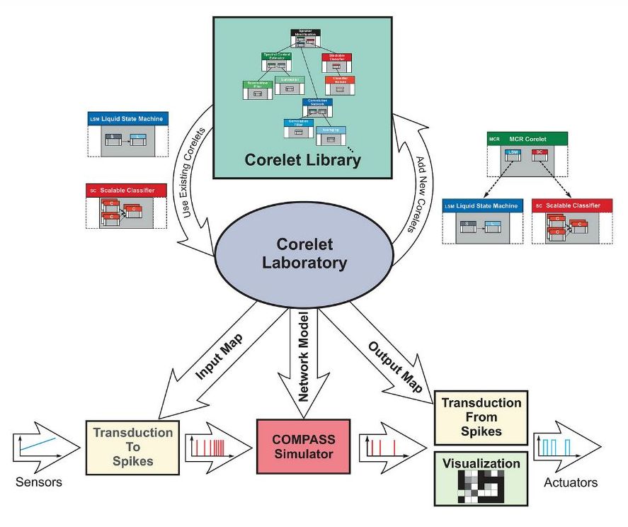
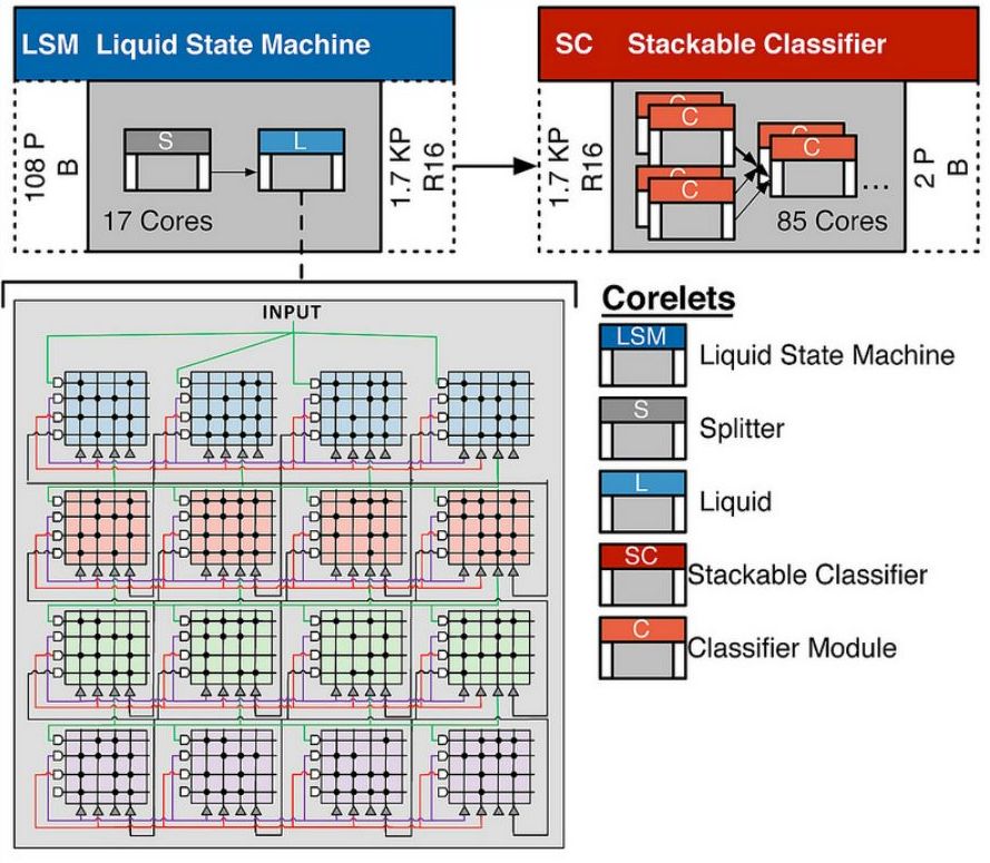
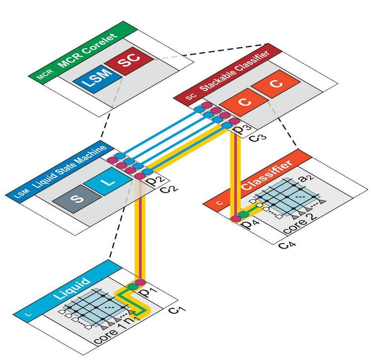
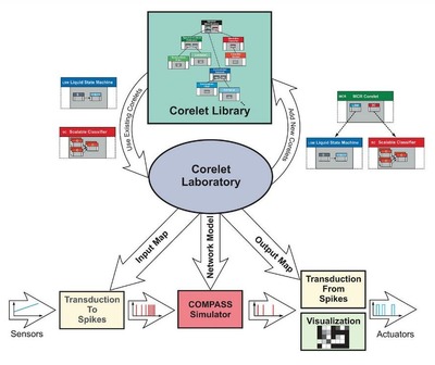
IBM researchers, led by Dharmendra S. Modha, have developed a programming language to enable the development of new sensory-based cognitive computing applications.
The new software ecosystem supports all aspects of the programming cycle - from design through development, debugging and deployment - and could enable a new generation of applications that mimic the brain's abilities for perception, action and cognition.
Courtesy of IBM |
| |
Armonk, N.Y., USA - July 10, 2014
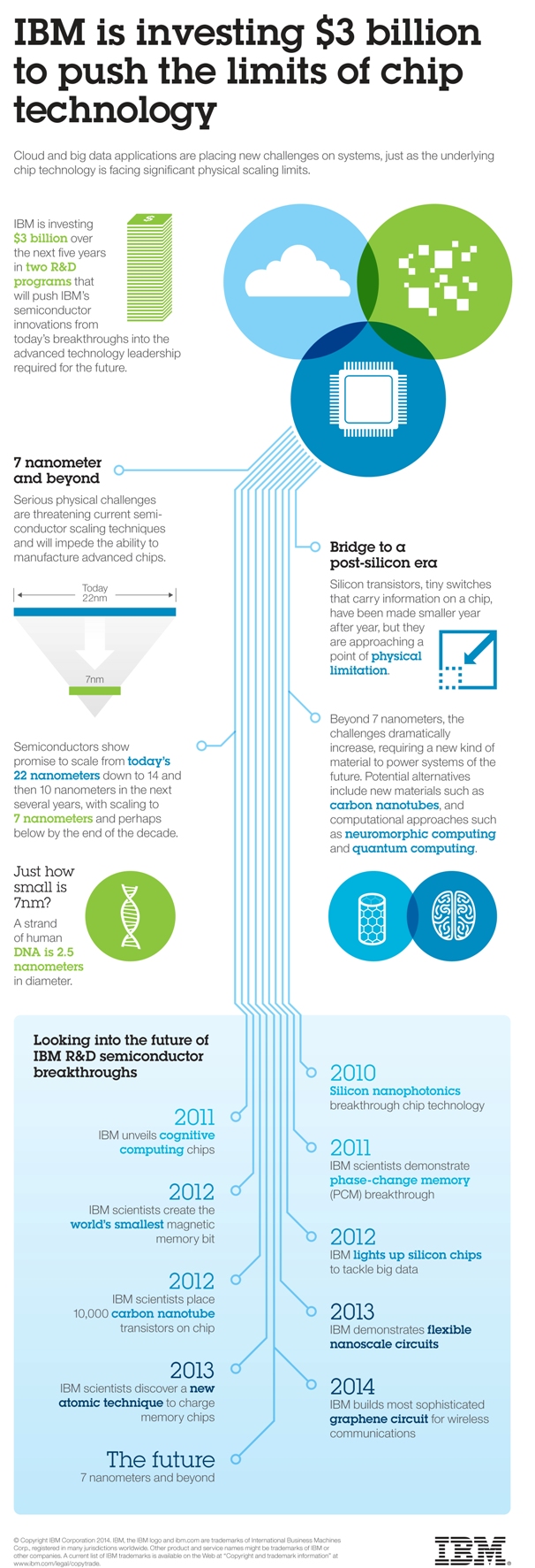
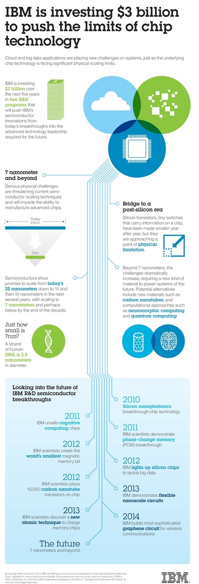
• Scientists and engineers to push limits of silicon technology to 7 nanometers and below and create post-silicon future
IBM (NYSE: IBM) today
announced it is investing $3 billion over the next 5 years in two broad research and early stage development programs to push the limits of chip technology needed to meet the emerging demands of cloud computing and Big Data systems.
These investments will push IBM's semiconductor innovations from today’s breakthroughs into the advanced technology leadership required for the future.
 |
| Courtesy of IBM |
| |
The first research program is aimed at so-called “
7 nanometer and beyond” silicon technology that will address serious physical challenges that are threatening current semiconductor scaling techniques and will impede the ability to manufacture such chips.
The second is focused on
developing alternative technologies for post-silicon era chips using entirely different approaches, which IBM scientists and other experts say are required because of the physical limitations of silicon based semiconductors.
Cloud and big data applications are placing new challenges on systems, just as the underlying chip technology is facing numerous significant physical scaling limits.
Bandwidth to memory, high speed communication and device power consumption are becoming increasingly challenging and critical.
 |
The new software ecosystem supports all aspects of the programming cycle - from design through development, debugging and deployment - and could enable a new generation of applications that mimic the brain's abilities for perception, action and cognition.
Courtesy of IBM |
| |
The teams will comprise IBM Research scientists and engineers from Albany and Yorktown, New York; Almaden, California; and Europe.
In particular,
IBM will be investing significantly in emerging areas of research that are already underway at IBM such as carbon nanoelectronics, silicon photonics, new memory technologies, and architectures that support quantum and cognitive computing.
These teams will focus on providing orders of magnitude improvement in system level performance and energy efficient computing.
 |
The new software ecosystem supports all aspects of the programming cycle - from design through development, debugging and deployment - and could enable a new generation of applications that mimic the brain's abilities for perception, action and cognition.
Courtesy of IBM |
| |
In addition,
IBM will continue to invest in the nanosciences and quantum computing--two areas of fundamental science where IBM has remained a pioneer for over three decades.
7 nanometer technology and beyond
IBM Researchers and other semiconductor experts predict that while challenging, semiconductors show promise to scale from today's 22 nanometers down to 14 and then 10 nanometers in the next several years.
However, scaling to 7 nanometers and perhaps below, by the end of the decade will require significant investment and innovation in semiconductor architectures as well as invention of new tools and techniques for manufacturing.
 |
The new software ecosystem supports all aspects of the programming cycle - from design through development, debugging and deployment - and could enable a new generation of applications that mimic the brain's abilities for perception, action and cognition.
Courtesy of IBM |
| |
"The question is not if we will introduce 7 nanometer technology into manufacturing, but rather how, when, and at what cost?" said
John Kelly, senior vice president, IBM Research.
"IBM engineers and scientists, along with our partners, are well suited for this challenge and are already working on the materials science and device engineering required to meet the demands of the emerging system requirements for cloud, big data, and cognitive systems. This new investment will ensure that we produce the necessary innovations to meet these challenges."
 |
The new software ecosystem supports all aspects of the programming cycle - from design through development, debugging and deployment - and could enable a new generation of applications that mimic the brain's abilities for perception, action and cognition.
Courtesy of IBM |
| |
"Scaling to 7nm and below is a terrific challenge, calling for deep physics competencies in processing nano materials affinities and characteristics. IBM is one of a very few companies who has repeatedly demonstrated this level of science and engineering expertise," said
Richard Doherty, technology research director, The Envisioneering Group.
Bridge to a “Post-Silicon” Era
Silicon transistors, tiny switches that carry information on a chip, have been made smaller year after year, but they are approaching a point of physical limitation.
Their increasingly small dimensions, now reaching the nanoscale, will prohibit any gains in performance due to the nature of silicon and the laws of physics.
Within a few more generations, classical scaling and shrinkage will no longer yield the sizable benefits of lower power, lower cost and higher speed processors that the industry has become accustomed to.
 |
IBM researchers, led by Dharmendra S. Modha, have developed a programming language to enable the development of new sensory-based cognitive computing applications.
The new software ecosystem supports all aspects of the programming cycle - from design through development, debugging and deployment - and could enable a new generation of applications that mimic the brain's abilities for perception, action and cognition.
Courtesy of IBM |
| |
With virtually all electronic equipment today built on
complementary metal–oxide–semiconductor (CMOS) technology, there is an urgent need for new materials and circuit architecture designs compatible with this engineering process as the technology industry nears physical scalability limits of the silicon transistor.
Beyond 7 nanometers, the challenges dramatically increase, requiring a new kind of material to power systems of the future, and new computing platforms to solve problems that are unsolvable or difficult to solve today.
Potential alternatives include new materials such as carbon nanotubes, and non-traditional computational approaches such as neuromorphic computing, cognitive computing, machine learning techniques, and the science behind quantum computing.
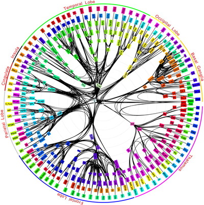 |
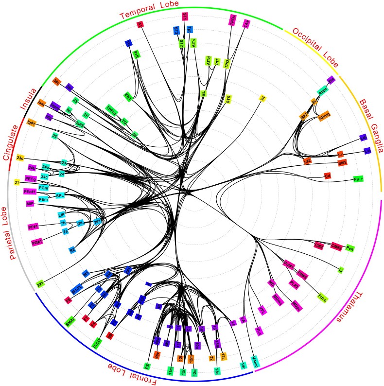
Macaque brain long-distance network.
Courtesy of IBM |
| |
As the leader in advanced schemes that point beyond traditional silicon-based computing, IBM holds over 500 patents for technologies that will drive advancements at 7nm and beyond silicon - more than twice the nearest competitor.
These continued investments will accelerate the invention and introduction into product development for IBM's highly differentiated computing systems for cloud, and big data analytics.
Several exploratory research breakthroughs that could lead to major advancements in delivering dramatically smaller, faster and more powerful computer chips, include quantum computing, neurosynaptic computing, silicon photonics, carbon nanotubes, III-V technologies, low power transistors and grapheme.
Quantum Computing
The most basic piece of information that a typical computer understands is a bit.
Much like a light that can be switched on or off, a bit can have only one of two values: "1" or "0.”
Described as superposition, this special property of qubits enables quantum computers to weed through millions of solutions all at once, while desktop PCs would have to consider them one at a time.
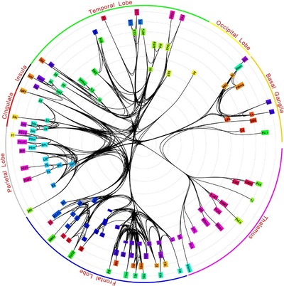 |
Innermost core for the undirected version of our network.
Courtesy of IBM |
| |
IBM is a world leader in superconducting qubit-based quantum computing science and is a pioneer in the field of experimental and theoretical quantum information, fields that are still in the category of fundamental science - but one that, in the long term, may allow the solution of problems that are today either impossible or impractical to solve using conventional machines.
The team recently demonstrated the first experimental realization of parity check with three superconducting qubits, an essential building block for one type of quantum computer.
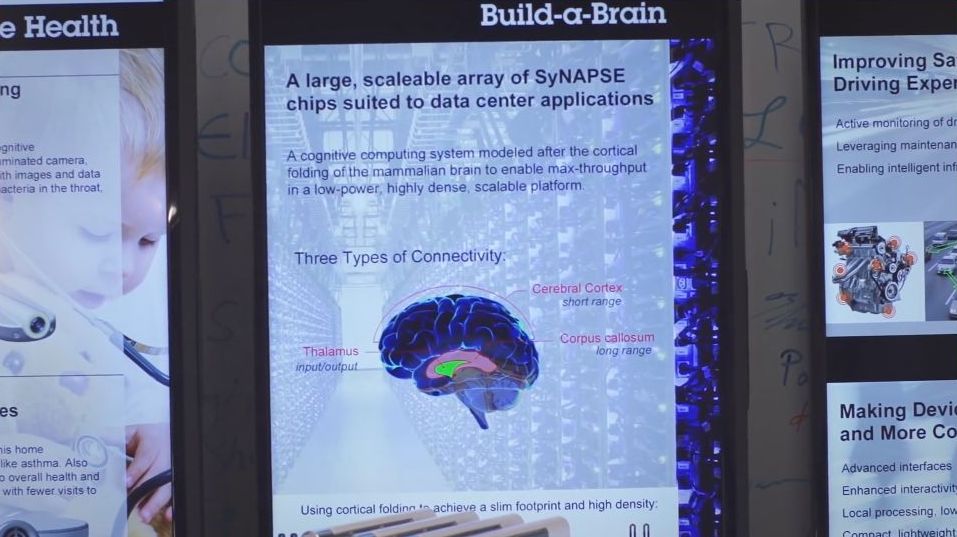
Neurosynaptic Computing
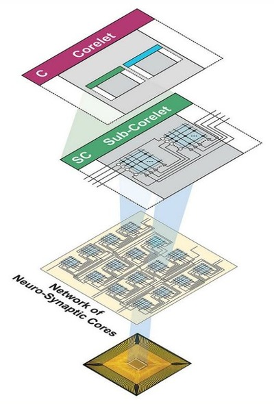
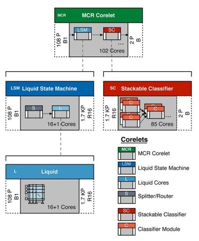
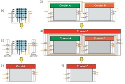
Bringing together nanoscience, neuroscience, and supercomputing, IBM and university partners have developed an end-to-end ecosystem including a novel non-von Neumann architecture, a new programming language, as well as applications.
This novel technology allows for computing systems that emulate the brain's computing efficiency, size and power usage.
 |
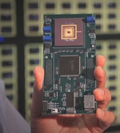
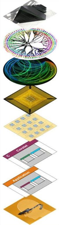
Chip Grand Challenge
R&D investment to push limits of silicon to meet demands of cloud computing and big data systems.
Courtesy of IBM |
| |
IBM’s long-term goal is to build a neurosynaptic system with ten billion neurons and a hundred trillion synapses, all while consuming only one kilowatt of power and occupying less than two liters of volume.
Silicon Photonics
IBM has been a pioneer in the area of CMOS integrated silicon photonics for over 12 years, a technology that integrates functions for optical communications on a
silicon chip, and the IBM team has recently designed and fabricated the world's first monolithic silicon photonics based transceiver with wavelength division multiplexing.
Such transceivers will use light to transmit data between different components in a computing system at high data rates, low cost, and in an energetically efficient manner.
 |
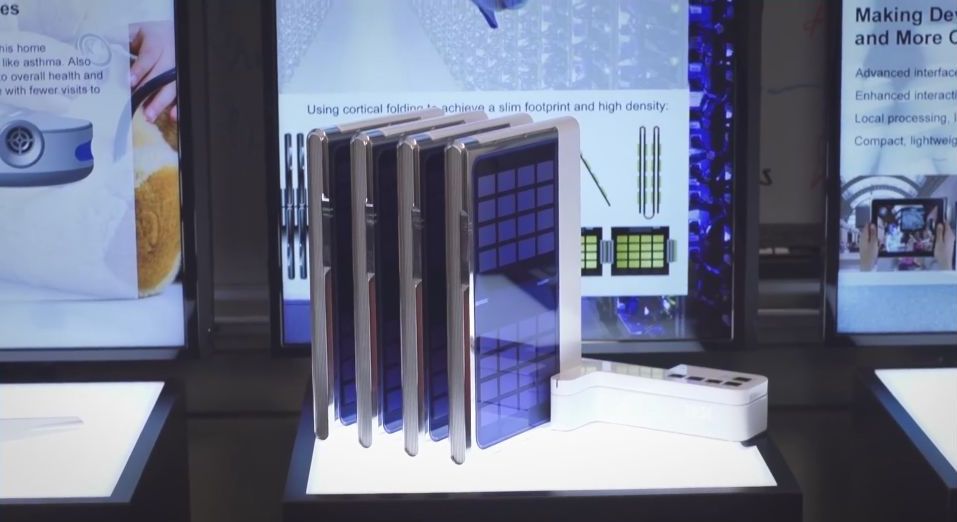
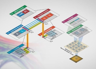
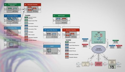
Scientists from IBM unveiled a breakthrough software ecosystem designed for programming silicon chips that have an architecture inspired by the function, low power, and compact volume of the brain.
The technology could enable a new generation of intelligent sensor networks that mimic the brain’s abilities for perception, action, and cognition.
Courtesy of IBM |
| |
Silicon nanophotonics takes advantage of pulses of light for communication rather than traditional copper wiring and provides a super highway for large volumes of data to move at rapid speeds between computer chips in servers, large datacenters, and supercomputers, thus alleviating the limitations of congested data traffic and high-cost traditional interconnects.
Businesses are entering a new era of computing that requires systems to process and analyze, in real-time, huge volumes of information known as
Big Data.
Silicon nanophotonics technology provides answers to Big Data challenges by seamlessly connecting various parts of large systems, whether few centimeters or few kilometers apart from each other, and move terabytes of data via pulses of light through optical fibers.
III-V technologies
IBM researchers have demonstrated the world’s highest transconductance on a self-aligned III-V channel metal-oxide semiconductor (MOS) field-effect transistors (FETs) device structure that is compatible with CMOS scaling.
These materials and structural innovation are expected to pave path for technology scaling at 7nm and beyond.
 |
Scientists from IBM unveiled a breakthrough software ecosystem designed for programming silicon chips that have an architecture inspired by the function, low power, and compact volume of the brain.
The technology could enable a new generation of intelligent sensor networks that mimic the brain’s abilities for perception, action, and cognition.
Courtesy of IBM |
| |
With more than an order of magnitude higher electron mobility than silicon,
integrating III-V materials into CMOS enables higher performance at lower power density, allowing for an extension to power/performance scaling to meet the demands of cloud computing and big data systems.
Carbon Nanotubes
IBM Researchers are working in the area of carbon nanotube (CNT) electronics and exploring whether CNTs can replace silicon beyond the 7 nm node.
As part of its activities for developing carbon nanotube based CMOS VLSI circuits, IBM recently demonstrated - for the first time in the world - 2-way CMOS NAND gates using 50 nm gate length carbon nanotube transistors.
 |
Scientists from IBM unveiled a breakthrough software ecosystem designed for programming silicon chips that have an architecture inspired by the function, low power, and compact volume of the brain.
The technology could enable a new generation of intelligent sensor networks that mimic the brain’s abilities for perception, action, and cognition.
Courtesy of IBM |
| |
IBM also has demonstrated the capability for purifying carbon nanotubes to 99.99 percent, the highest (verified) purities demonstrated to date, and transistors at 10 nm channel length that show no degradation due to scaling - this is unmatched by any other material system to date.
Carbon nanotubes are single atomic sheets of carbon rolled up into a tube.
The carbon nanotubes form the core of a transistor device that will work in a fashion similar to the current silicon transistor, but will be better performing.
They could be used to replace the transistors in chips that power data-crunching servers, high performing computers and ultra fast smart phones.
 |
Scientists from IBM unveiled a breakthrough software ecosystem designed for programming silicon chips that have an architecture inspired by the function, low power, and compact volume of the brain.
The technology could enable a new generation of intelligent sensor networks that mimic the brain’s abilities for perception, action, and cognition.
Courtesy of IBM |
| |
Carbon nanotube transistors can operate as excellent switches at molecular dimensions of less than ten nanometers – the equivalent to 10,000 times thinner than a strand of human hair and less than half the size of the leading silicon technology.
Comprehensive modeling of the electronic circuits suggests that about a five to ten times improvement in performance compared to silicon circuits is possible.
Graphene
Graphene is pure carbon in the form of a one atomic layer thick sheet. It is an excellent conductor of heat and electricity, and it is also remarkably strong and flexible.
Electrons can move in graphene about ten times faster than in commonly used semiconductor materials such as silicon and silicon germanium.
Its characteristics offer the possibility to build faster switching transistors than are possible with conventional semiconductors, particularly for applications in the handheld wireless communications business where it will be a more efficient switch than those currently used.
 |
Scientists from IBM unveiled a breakthrough software ecosystem designed for programming silicon chips that have an architecture inspired by the function, low power, and compact volume of the brain.
The technology could enable a new generation of intelligent sensor networks that mimic the brain’s abilities for perception, action, and cognition.
Courtesy of IBM |
| |
Recently in 2013, IBM demonstrated the world's first graphene based integrated circuit receiver front end for wireless communications.
The circuit consisted of a 2-stage amplifier and a down converter operating at 4.3 GHz.
Next Generation Low Power Transistors
In addition to new materials like
CNTs, new architectures and innovative device concepts are required to boost future system performance.
Power dissipation is a fundamental challenge for
nanoelectronic circuits.
To explain the challenge, consider a leaky water faucet - even after closing the valve as far as possible water continues to drip - this is similar to today’s transistor, in that energy is constantly "leaking" or being lost or wasted in the off-state.
A potential alternative to today’s power hungry silicon field effect transistors are so-called steep slope devices.
They could operate at much lower voltage and thus dissipate significantly less power.
 |
Scientists from IBM unveiled a breakthrough software ecosystem designed for programming silicon chips that have an architecture inspired by the function, low power, and compact volume of the brain.
The technology could enable a new generation of intelligent sensor networks that mimic the brain’s abilities for perception, action, and cognition.
Courtesy of IBM |
| |
IBM scientists are researching tunnel field effect transistors (TFETs).
In this special type of transistors the quantum-mechanical effect of band-to-band tunneling is used to drive the current flow through the transistor.
TFETs could achieve a 100-fold power reduction over complementary CMOS transistors, so integrating TFETs with CMOS technology could improve low-power integrated circuits.
Recently,
IBM has developed a novel method to integrate III-V nanowires and heterostructures directly on standard silicon substrates and built the
first ever InAs/Si tunnel diodes and
TFETs using InAs as source and Si as channel with wrap-around gate as steep slope device for low power consumption applications.
"In the next ten years computing hardware systems will be fundamentally different as our scientists and engineers push the limits of semiconductor innovations to explore the post-silicon future," said
Tom Rosamilia, senior vice president, IBM Systems and Technology Group.
"IBM Research and Development teams are creating breakthrough innovations that will fuel the next era of computing systems."
 |
Scientists from IBM unveiled a breakthrough software ecosystem designed for programming silicon chips that have an architecture inspired by the function, low power, and compact volume of the brain.
The technology could enable a new generation of intelligent sensor networks that mimic the brain’s abilities for perception, action, and cognition.
Courtesy of IBM |
| |
IBM's historic contributions to silicon and
semiconductor innovation include the invention and/or first implementation of: the single cell DRAM, the “Dennard scaling laws” underpinning "Moore's Law", chemically amplified photoresists, copper interconnect wiring, Silicon on Insulator, strained engineering, multi core microprocessors, immersion lithography, high speed silicon germanium (SiGe), High-k gate dielectrics, embedded DRAM, 3D chip stacking, and Air gap insulators.
IBM researchers also are credited with initiating the era of nano devices following the
Nobel prize winning invention of the scanning tunneling microscope which enabled nano and atomic scale invention and innovation.
IBM will also continue to fund and collaborate with university researchers to explore and develop the future technologies for the semiconductor industry.
In particular,
IBM will continue to support and fund university research through private-public partnerships such as the NanoElectornics Research Initiative (NRI), and the Semiconductor Advanced Research Network (STARnet), and the Global Research Consortium (GRC) of the Semiconductor Research Corporation.
Contacts information
Steve Tomasco
IBM Media Relations
917-687-4588
stomasc@us.ibm.com
Ari Entin
IBM Media Relations
408-927-2272
aentin@us.ibm.com
Video
A new software ecosystem for cognitive systems
https://www.youtube.com/watch?v=J69EJxUr8mw
Source: IBM
http://www-03.ibm.com/press/us/en/index.wss
ASTROMAN Magazine - 2014.07.08
City of Madrid Implements IBM's Large Smarter Cities Environmental Analytics Project
http://www.astroman.com.pl/index.php?mod=magazine&a=read&id=1751
ASTROMAN Magazine - 2014.06.27
Qatar Public Works Authority 'Ashghal' Selects IBM for Smarter Infrastructure
https://www.astroman.com.pl/index.php?mod=magazine&a=read&id=1741
ASTROMAN Magazine - 2014.05.11
Report: IBM Named #1 Preferred Provider of IaaS Cloud by Enterprises
http://www.astroman.com.pl/index.php?mod=magazine&a=read&id=1710
ASTROMAN Magazine - 2014.03.15
Keynote trends at CeBIT 2014
http://www.astroman.com.pl/index.php?mod=magazine&a=read&id=1675
ASTROMAN Magazine – 2014.02.25
GSMA Announces Winners of the 2014 Global Mobile Awards
http://www.astroman.com.pl/index.php?mod=magazine&a=read&id=1664
ASTROMAN Magazine – 2014.02.01
IBM and Twitter Announce Patent and Cross-License Agreement. Twitter purchases 900 patents from IBM
http://www.astroman.com.pl/index.php?mod=magazine&a=read&id=1648
ASTROMAN Magazine - 2013.12.22
IBM to Acquire Aspera to Help Companies Speed Global Movement of Big Data
http://www.astroman.com.pl/index.php?mod=magazine&a=read&id=1610
ASTROMAN Magazine - 2013.11.16
IBM Watson's Next Venture: Fueling New Era of Cognitive Apps Built in the Cloud by Developers
http://www.astroman.com.pl/index.php?mod=magazine&a=read&id=1587
ASTROMAN Magazine - 2013.10.26
President Barack Obama to Visit IBM'S P-TECH School in Brooklyn, NY, USA
http://www.astroman.com.pl/index.php?mod=magazine&a=read&id=1576
ASTROMAN Magazine - 2013.09.21
IBM Acquires Daeja Image Systems Ltd.
http://www.astroman.com.pl/index.php?mod=magazine&a=read&id=1557
ASTROMAN Magazine - 2013.09.01
IBM Closes Acquisition of CSL International
http://www.astroman.com.pl/index.php?mod=magazine&a=read&id=1541
ASTROMAN Magazine – 2013.08.17
IBM to Acquire Trusteer to Help Companies Combat Financial Fraud and Advanced Security Threats
http://www.astroman.com.pl/index.php?mod=magazine&a=read&id=1519
ASTROMAN Magazine – 2013.08.17
IBM Awarded 10 Year US$1 Billion Cloud Hosting Services Contract
http://www.astroman.com.pl/index.php?mod=magazine&a=read&id=1518
ASTROMAN Magazine – 2013.08.10
Google, IBM, Mellanox, NVIDIA, Tyan Announce Development Group for Data Centers
http://www.astroman.com.pl/index.php?mod=magazine&a=read&id=1511
ASTROMAN Magazine – 2013.04.13
Gartner Report: IBM Named Marketshare Leader
http://www.astroman.com.pl/index.php?mod=magazine&a=read&id=1441
ASTROMAN Magazine – 2013.04.08
IBM To Open Cloud Lab For Wall Street Clients
http://www.astroman.com.pl/index.php?mod=magazine&a=read&id=1440
ASTROMAN Magazine – 2013.04.07
IBM: ICM's New Blue Gene Supercomputer Supports The Largest Biomedical Research Initiative In Poland
http://www.astroman.com.pl/index.php?mod=magazine&a=read&id=1437
ASTROMAN Magazine - 2013.03.17
IBM Opens Lab to Bring R&D to the CEO
http://www.astroman.com.pl/index.php?mod=magazine&a=read&id=1426
ASTROMAN Magazine - 2013.02.24
Deutsche Telekom and IBM Collaborate to Help Build Smarter Cities
http://www.astroman.com.pl/index.php?mod=magazine&a=read&id=1413
ASTROMAN Magazine - 2013.01.18
IBM Research Team Wins Coveted Feynman Prize for Advancing Scanning Probe Microscopy
http://www.astroman.com.pl/index.php?mod=magazine&a=read&id=1391
ASTROMAN Magazine - 2012.12.15
Made in IBM Labs: IBM Lights Up Silicon Chips to Tackle Big Data
http://www.astroman.com.pl/index.php?mod=magazine&a=read&id=1367
ASTROMAN Magazine - 2012.12.08
IBM Completes Acquisition of Kenexa for $1.3 billion
http://www.astroman.com.pl/index.php?mod=magazine&a=read&id=1362
ASTROMAN Magazine - 2012.11.18
IBM Makes $4 Billion in Financing Available for Business Partners; Announces New Mobile App to Speed Access to Credit within Minutes
http://www.astroman.com.pl/index.php?mod=magazine&a=read&id=1352
ASTROMAN Magazine - 2012.11.11
IBM Delivers New Software to Help Organizations Build Smarter Products
http://www.astroman.com.pl/index.php?mod=magazine&a=read&id=1347
ASTROMAN Magazine - 2012.10.07
IBM Completes Acquisition of Texas Memory Systems
http://www.astroman.com.pl/index.php?mod=magazine&a=read&id=1325
ASTROMAN Magazine - 2012.09.29
Virginia M. Rometty Elected IBM Chairman
http://www.astroman.com.pl/index.php?mod=magazine&a=read&id=1319
ASTROMAN Magazine – 2012.05.02
New IBM Business Integration Software Helps Enterprises Accelerate Adoption of Social Business, Cloud and Mobile Technologies
http://www.astroman.com.pl/index.php?mod=magazine&a=read&id=1231
ASTROMAN Magazine – 2012.04.01
IBM Increases Presence in Poland with New Branch Offices
http://www.astroman.com.pl/index.php?mod=magazine&a=read&id=1213
Editor-in-Chief of ASTROMAN magazine: Roman Wojtala, PhD.
 subskrypcja RSS